The Atomic Force Microscope (AFM) is a high-resolution scanning probe microscopy technique, co-invented by Gerd Binnig, Heinrich Rohrer, and Calvin Quate in 1986. AFM uses the interaction forces between a sharp probe on a microcantilever and the sample surface to detect the surface topography and physical properties of the sample, with atomic-level resolution.
The atomic force microscope (AFM) secures one end of a highly sensitive microcantilever, with a tiny probe tip at the other end that gently contacts the sample surface. Due to the extremely weak repulsive forces between the atoms at the tip of the probe and the atoms on the sample surface, by controlling the constancy of this force during scanning, the microcantilever with the probe tip will oscillate vertically above the sample surface, corresponding to the equipotential surface of the interaction forces between the probe tip and the atoms on the sample surface. Using optical detection or tunneling current detection methods, the positional changes of the microcantilever corresponding to each scanning point can be measured, thereby obtaining information about the surface topography of the sample.
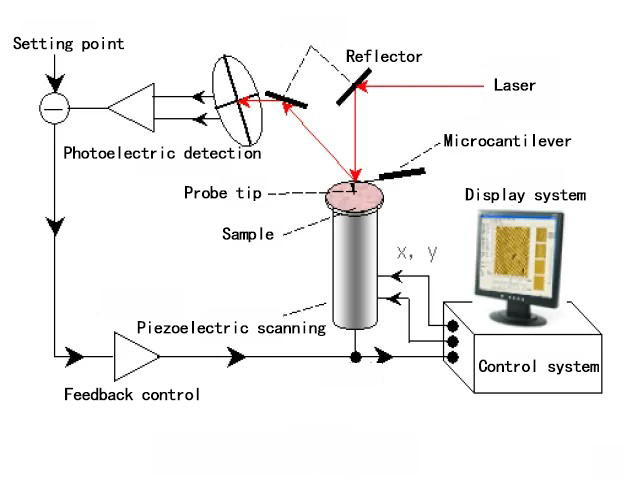
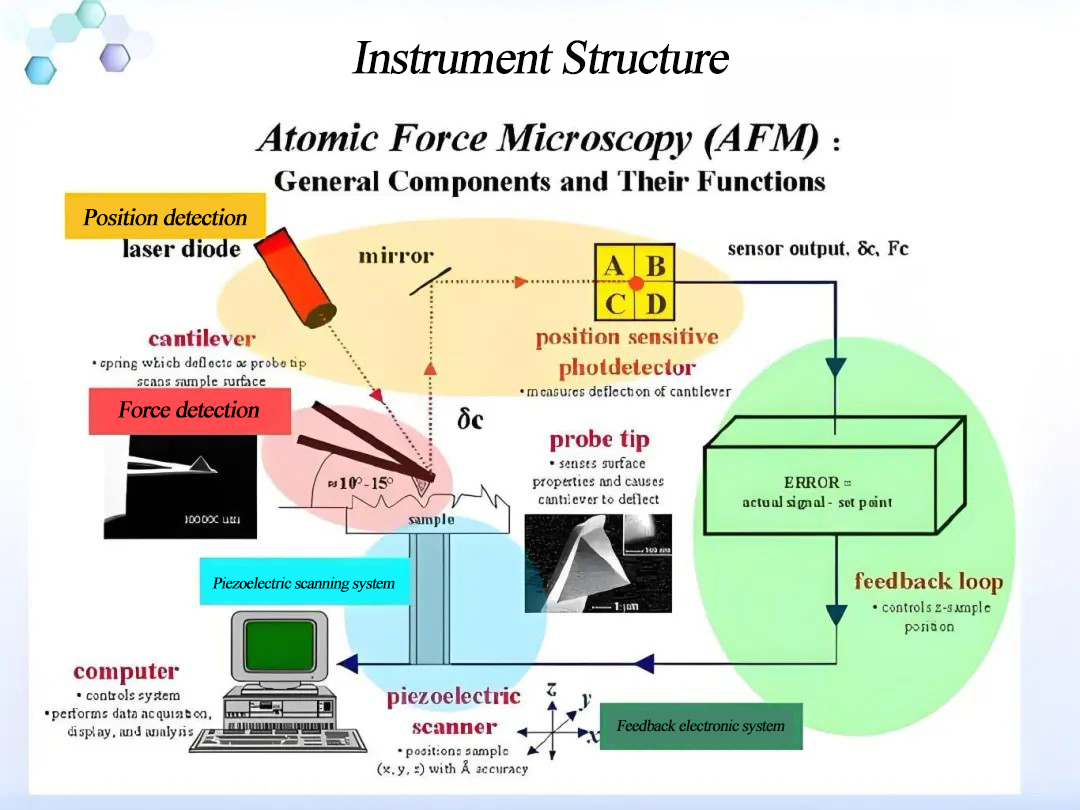
The main components of an atomic force microscope include the probe, probe positioning and scanning mechanisms, force detection sections, and feedback control units. The probe material should be a harder metal, with tungsten wire being the most commonly used material. After electrochemical etching and focused ion beam milling, probes with a smaller tip radius can be obtained.
AFM has three basic imaging modes:
● Contact mode: The probe tip is in soft "actual contact" with the sample. As the tip gently scans across the sample surface, the contact force causes the cantilever to bend, thereby obtaining the surface profile of the sample.
● Non-contact mode: In non-contact mode, the tip vibrates above the sample surface without ever coming into contact with it. The detector measures long-range forces such as van der Waals forces and electrostatic forces that do not damage the sample being images.
● Tapping mode: In tapping mode, the tip vibrates at a certain frequency and amplitude above the sample surface, never coming into contact with it. The detector senses changes in the resonance frequency and amplitude of the tip's forced vibration, thereby obtaining information about the sample's surface topography.
● High spatial resolution: AFM can provide atomic-level spatial resolution, and under ideal conditions, it is possible to observe the arrangement and structure of individual atoms.
● Non-destructive measurement: The measurement process of AFM is non-destructive, which means that the sample is not altered or damaged during the measurement, making it particularly important for studying fragile biological samples and soft matter.
● Wide applicability to samples: AFM can be used for various types of samples, including conductive and non-conductive materials, solid and liquid environments, as well as samples at room temperature and low temperatures.
● Versatility: AFM is not only used for topographic imaging but also for measuring mechanical properties (such as hardness, elastic modulus) and characterizing electrical properties (such as conductivity and local potential).
● Dynamic and static measurements: AFM can perform dynamic (such as tapping mode) and static (such as contact mode) measurements, making it adaptable to different measurement requirements and sample characteristics.
● Environmental adaptability: AFM can operate under various environmental conditions, including high humidity, high temperature, low temperature, and various chemical atmospheres, making it very useful in materials science and industrial applications.
● Simple sample preparation: Compared to some characterization techniques that require complex sample preparation, AFM typically does not require a complicated sample preparation process.
● Compatibility with other techniques: AFM can be used in conjunction with other characterization techniques, such as Raman spectroscopy, infrared spectroscopy, etc., to provide more comprehensive sample information.
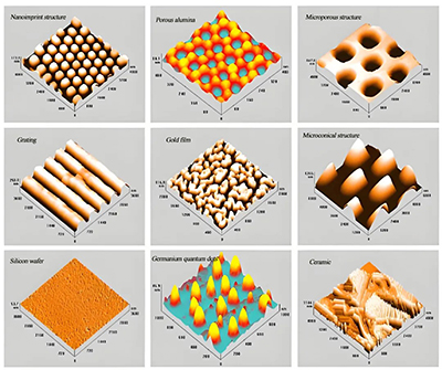
AFM images of materials with large surface to volume ratio
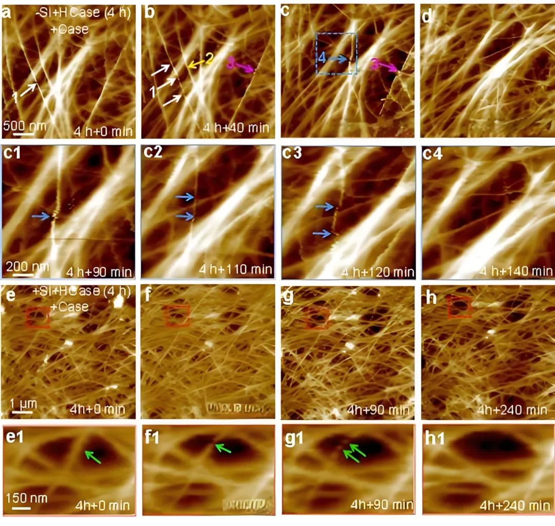
In situ AFM observation of cellulase


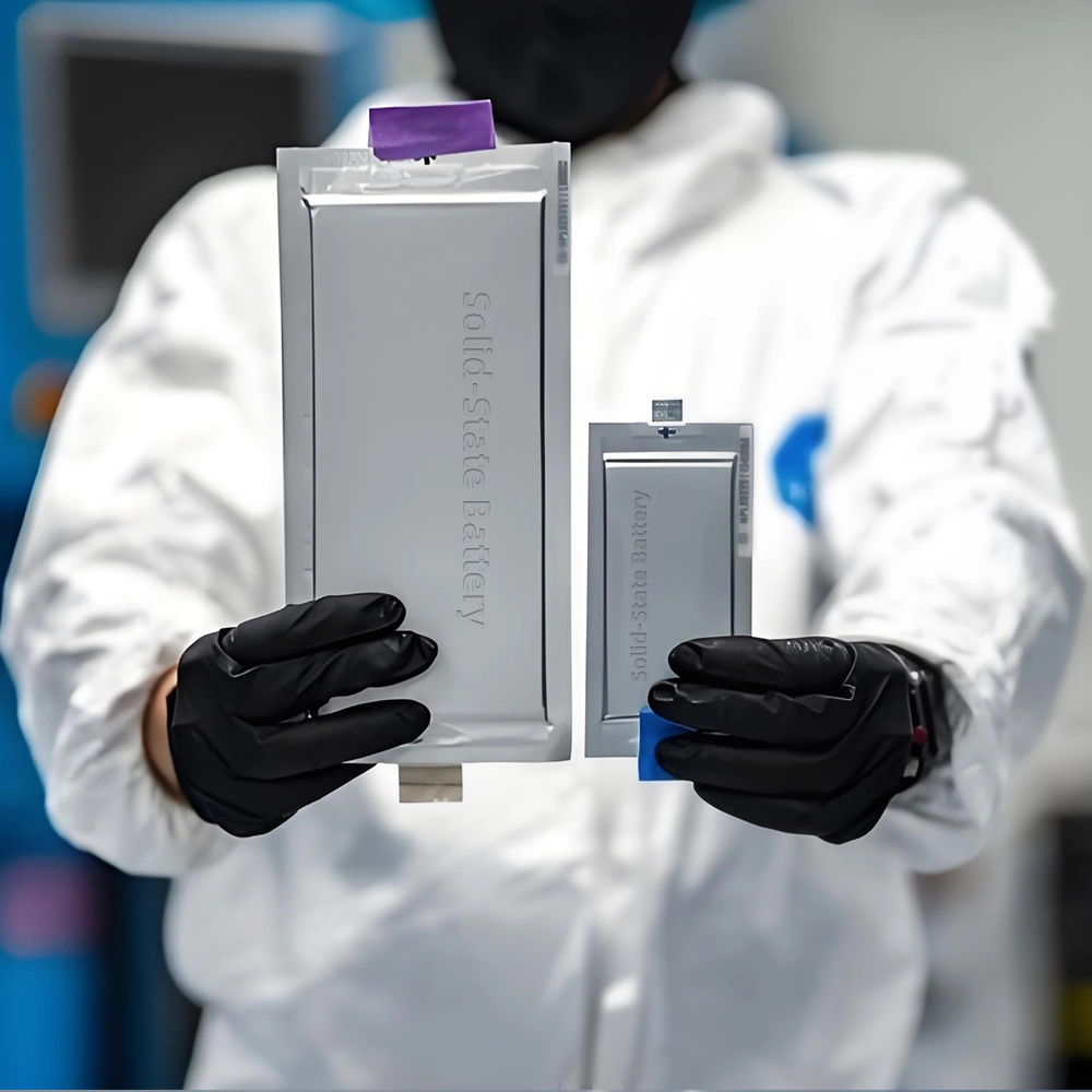
The lab focuses on solid-state battery research to overcome traditional lithium batteries' safety and energy density issues, supporting environmental sustainability. It develops innovative solid-state electrolytes, refines electrode materials, and investigates ion transfer and interface stability to revolutionize battery technology.

The electric vehicle battery industry is rapidly developing, focusing on technological innovation, market competition, and sustainability. Research hotspots include solid-state batteries, new types of electrolytes, BMS optimization, and recycling technologies. The environmental adaptability, safety, and economic viability of batteries are key research areas, and the industry is expected to undergo more innovation and transformation.
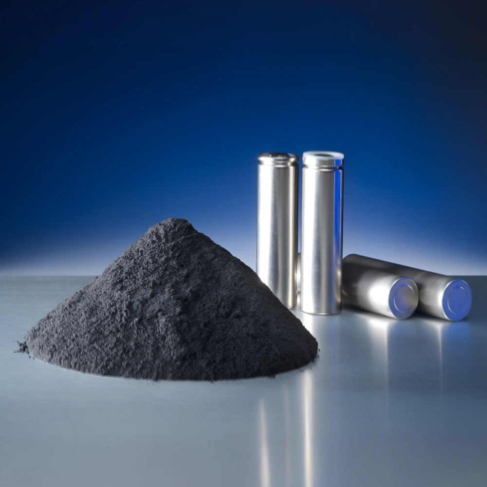
We specialize in battery preparation technology research, focusing on overcoming existing energy storage challenges by innovating in electrode materials, battery chemistry, and manufacturing processes to improve performance, enhance safety, and reduce costs. Sustainability and recycling technologies for batteries are also emphasized to mitigate environmental impacts and foster the growth of green energy.